The idea: a bubble is an inverter you can move
On a schematic, the small circle at a gate's pin is a bubble: an inverter squeezed onto the pin. NAND is an AND with a bubble on its output. Bubbles can be moved by two rules. Two bubbles in a row on one wire cancel. And De Morgan's law lets a bubble pass through a gate if the gate changes from AND to OR, or from OR to AND.
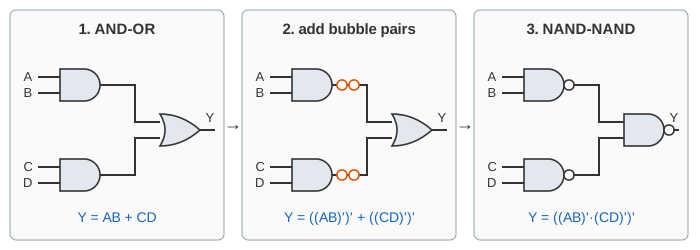
Moving bubbles around is called bubble pushing. It is used two ways: to rebuild a circuit from cheaper gates, and to read a circuit someone else drew. The canvas does both. Press Next Step to take one step. The panel on the right recomputes Y from the drawing on all 16 inputs after every step, so you can see that nothing changes.
The second half of the page is about wires that are not 0 or 1: a wire nobody drives (Z) and a wire two drivers fight over (X).
Two-level and multilevel logic
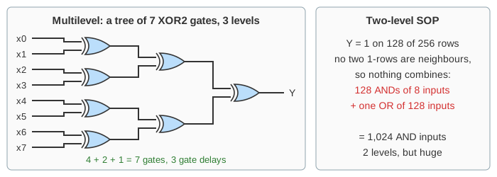
A sum of products (SOP) is two-level logic: a level of ANDs, then one OR. Any truth table can be written this way, and the Karnaugh map finds the smallest one. But two levels can be very large. An 8-input XOR (parity) is 1 for 128 of its 256 input rows, and no two of these rows are neighbours, so its minimal SOP has 128 terms of 8 inputs each.
Built as a tree of 2-input XOR gates, the same function needs only 7 gates in 3 levels. Circuits with more than two levels are multilevel. They are usually smaller, at the price of more gate delays on the longest path.
The bubble-pushing rules
| Rule | As algebra | On the schematic |
|---|---|---|
| Two bubbles cancel | (X')' = X | A bubble pair may be added to, or removed from, any wire |
| NAND = OR of inverted inputs | (AB)' = A' + B' | AND with output bubble = OR with input bubbles |
| NOR = AND of inverted inputs | (A + B)' = A'B' | OR with output bubble = AND with input bubbles |
Pushing a bubble backward through a gate, from the output to the inputs, swaps AND and OR and puts a bubble on every input. Pushing bubbles forward from all inputs works the same way in reverse.
AND-OR becomes NAND-NAND, OR-AND becomes NOR-NOR
Start with Y = AB + CD. Put a bubble pair on each wire between the two levels. Slide one bubble of each pair to the AND gate's output: the ANDs are now NANDs. The other bubble sits on an input of the OR. An OR with every input bubbled is a NAND. So any SOP can be built from NAND gates only, with the same structure. Demo: AND-OR → NAND-NAND.
The dual works for a product of sums: Y = (A + B)(C + D) becomes NOR-NOR. Demo: OR-AND → NOR-NOR.
Why bother? In CMOS, an inverting gate is the natural one: a NAND or NOR is a handful of transistors. An AND is a NAND followed by an inverter, so it is larger and slower. A NAND-NAND circuit has the same function in fewer transistors and fewer delays. The transistor page shows how a CMOS NAND is built.
Reading a circuit full of bubbles
To find what a drawn circuit computes, bubble-push until the bubbles cancel:
- Start at the output and work toward the inputs.
- If the output gate has a bubble on its output, redraw it with De Morgan so that the bubble moves to its inputs (unless you want Y').
- On each wire, try to have bubbles at both ends or at neither. A pair cancels.
- A lone bubble left on a wire is a complement: write that signal primed.
In Demo: read Y = AB + C'D', the circuit is NAND(NAND(A, B), OR(C, D)). The output NAND becomes an OR with bubbled inputs. Its top bubble meets the first NAND's output bubble and both go. The bottom one has no partner, so the OR's output is complemented: (C + D)' = C'D'. Result: Y = AB + C'D'.
Four values: 0, 1, Z and X
So far every wire is 0 or 1. Real circuits have two more cases, and simulators such as Verilog show them as letters.
| Value | Meaning | How it happens |
|---|---|---|
| 0, 1 | Driven low or high | Exactly one gate drives the wire, or several drive the same value |
| Z | High impedance, floating | No driver is connected: a tristate buffer is off, or an input pin is left unconnected |
| X | Unknown or illegal | Contention (one driver at 0, another at 1), a gate reading Z or X, or an uninitialized flip-flop in a simulator |
Tristate buffers and the shared bus
A tristate buffer has a data input A, an enable E and an output Y. With E = 1 it is a plain buffer: Y = A. With E = 0 its output transistors are both off, so Y is disconnected: Z. Several tristate buffers can then share one wire, a bus, as long as only one is enabled at a time. Old processor buses and memory chips with an output-enable pin work this way. Demo: bus, drivers take turns.
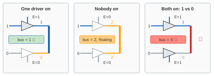
The table on the canvas is the resolution of two drivers: Z gives way to any value, equal values agree, and 0 against 1 is X. The reader on the right shows what happens next: a gate whose input is Z or X has an unknown output, so the unknown spreads to everything downstream.
Floating: Z
When nobody drives the bus, its voltage is whatever charge is left on it, drifting with leakage and noise. It is not a logic level. A floating input may read as 0 in one test and 1 in the next. It can also stop half way, where both transistors of the reading gate conduct a little and waste power. Demo: nobody drives (Z). Designers fix this with a weak pull-up or pull-down resistor, or a bus keeper that holds the last value, so the idle bus has a known value.
Contention: X
When two enabled drivers disagree, one connects the wire to the supply and the other to ground. The wire settles somewhere between, often in the forbidden zone, and a large current flows through both drivers. It wastes power, heats the chip and can damage it. Demo: contention, 1 vs 0 (X). If both drive the same value there is no fight (Both drive 1 in the bus select), but a design that relies on that is fragile: the enables should be mutually exclusive, for example from a decoder that turns on one line at a time.
Don't confuse this X with the X in a truth table or a Karnaugh map. There it means "don't care": the designer may choose 0 or 1. On a wire it means "can't tell", and it is a bug.
What the page leaves out
- Timing. Gates here switch at once. Multilevel circuits have longer paths; turning a driver off and another on at the same moment can still overlap briefly. See timing analysis.
- Electrical strength. Real drivers have different strengths, so a strong driver can win over a weak one (Verilog models this with drive strengths). Pull-ups and keepers are left out of the canvas.
- Inside the tristate buffer. In CMOS it is an inverter whose pull-up and pull-down transistors each get an extra transistor in series, both turned off when E = 0. The transistor page shows how CMOS gates are built.
- Multiplexers instead of buses. Modern chips rarely use on-chip tristate buses; a multiplexer picks one source without any risk of contention.
- Bigger circuits. Bubble pushing works the same for any number of gates and levels; synthesis tools do it automatically.
References
Harris and Harris, Digital Design and Computer Architecture, sections 2.5 (Multilevel Combinational Logic) and 2.6 (X's and Z's, Oh My)