The idea: a switch you work with a voltage
A light switch connects two wires when you press it. A transistor does the same, but it is worked by a voltage instead of a finger: the voltage on one terminal decides whether current can flow between the other two. Because the output of one transistor can drive the input of the next, switches can control switches, and that is all a digital computer is.
The page draws wires at 2.5 V or more in dark blue and lower wires in grey. A conducting channel is green, a half-on one orange, an open one white. Pick a circuit and an input voltage A (and B for the NAND), or press Truth Table to try every input, one row per step. The supply is VDD = 5 V; 0 V means logic 0 and 5 V logic 1.
The nMOS transistor: gate, threshold, channel
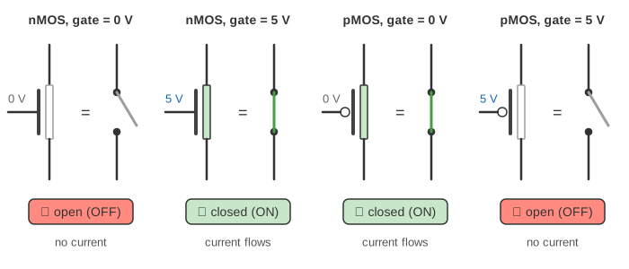
A MOSFET (metal-oxide-semiconductor field-effect transistor) has a gate, a source and a drain. The gate sits on a thin layer of glass (silicon dioxide), so no current flows into it. In an nMOS, a positive gate voltage pulls electrons to the surface under the gate. Once the gate is more than the threshold voltage Vth (1 V here) above the source, those electrons form a channel that connects source and drain.
In the nMOS switch a 1 kΩ lamp hangs from VDD, and the transistor connects its lower end to ground. With 0 V or 0.8 V on the gate there is no channel: no current, the lamp is dark, and Vout stays at 5 V. With 5 V on the gate the channel acts like a resistor of about 50 Ω: 4.76 mA flows, the lamp lights and Vout drops to 0.24 V (Demo: nMOS switch, 5 V on the gate turns it on). A 1 in gives a 0 out, so this one transistor is already an inverter.
Fully on, half on, off
Between the two ends, the transistor is neither open nor closed. Just above Vth the channel is thin and caps the current at k/2 · (VGS − Vth)², the saturation region (here k = 5 mA/V²). At 1.5 V on the gate only 0.76 mA gets through, so the lamp is dim and Vout = 4.24 V, still a 1. With a strong gate voltage the transistor is in the linear (triode) region and behaves like a small resistor (Demo: nMOS sweep, half on at 1.5 V).
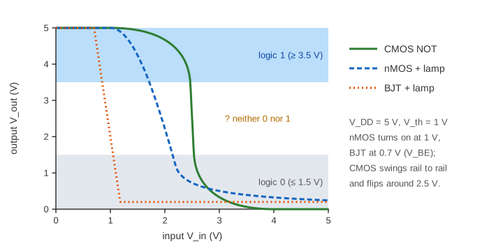
This is why logic uses only two voltage ranges. Here anything at or below 1.5 V counts as 0 and anything at or above 3.5 V as 1. A gate whose output lands in between (orange boxes on the canvas) would be read differently by different gates downstream.
The BJT: current in, current out
A bipolar junction transistor (BJT) has a base, a collector and an emitter. It is controlled by current, not voltage. The base-emitter junction is a diode, so nothing flows until the base is about VBE = 0.7 V above the emitter. Then the base current IB = (Vin − 0.7 V) / RB lets through a collector current β · IB, here with β = 100.
- Cutoff (Vin below 0.7 V): no base current, no collector current. Switch open.
- Active: at 0.8 V, IB = 0.01 mA and IC = 1 mA, so Vout = 4 V. The transistor amplifies; it is not a switch yet.
- Saturation: at 5 V, IB = 0.43 mA asks for 43 mA, but the lamp allows only 4.8 mA. The transistor is fully on with VCE = 0.2 V. Switch closed (Demo: BJT, the base current decides).
| MOSFET | BJT | |
|---|---|---|
| controlled by | gate voltage VGS | base current IB |
| turns on at | Vth, about 0.3–1 V | VBE ≈ 0.7 V |
| input current when on | 0 (insulated gate) | IB flows all the time |
| "fully on" voltage drop | I · Ron, can be millivolts | VCE(sat) ≈ 0.2 V |
| used for | almost every chip (CMOS), power switches | analog amplifiers, older logic (TTL), some power stages |
pMOS and the CMOS inverter
The nMOS switch has a weakness: when it is on, current flows through the lamp (or a pull-up resistor) all the time. A pMOS transistor is the mirror image of an nMOS: it conducts when its gate is at least Vth below its source, so a pMOS with its source on VDD is on when the input is 0. CMOS (complementary MOS) puts a pMOS between VDD and the output and an nMOS between the output and ground, with both gates on the input.
- A = 0 V: the pMOS is on, the nMOS off. Y is connected to VDD: Y = 5 V = 1.
- A = 5 V: the pMOS is off, the nMOS on. Y is connected to ground: Y = 0 V = 0.
In both cases one switch is open, so no current flows from VDD to ground (Demo: CMOS NOT, one transistor on at a time). A CMOS gate uses power only while it switches. That is why a phone chip with billions of transistors does not melt. During the switch, for inputs between 1 V and 4 V, both transistors conduct at once: at 2.5 V a short-circuit current of 6.33 mA flows straight through (Demo: CMOS NOT sweep, both on in the middle). Real gates pass through this zone quickly.
The CMOS NAND: series and parallel
For two inputs, CMOS uses the rule: switches in series make AND, switches in parallel make OR. The NAND has two nMOS in series as the pull-down: Y is pulled to 0 only if A and B are both 1. It has two pMOS in parallel as the pull-up: Y is pulled to 1 if A or B is 0. The two networks are exact complements, so for every input exactly one of them conducts (Demo: CMOS NAND truth table).
| A | B | pull-up (pMOS ∥) | pull-down (nMOS in series) | Y |
|---|---|---|---|---|
| 0 | 0 | both on | open | 1 |
| 0 | 1 | pMOS A on | open | 1 |
| 1 | 0 | pMOS B on | open | 1 |
| 1 | 1 | open | both on | 0 |
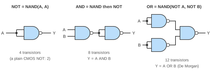
The same rule swapped gives a NOR: nMOS in parallel, pMOS in series. CMOS gates naturally invert, so an AND gate is a NAND followed by a NOT: 6 transistors instead of 4.
From NAND to every gate
NAND is universal: every logic function can be built from NAND gates alone. Tie both inputs together and it is a NOT. Add a NOT after it and it is an AND. Invert both inputs first and De Morgan's law turns it into an OR.
From here the next level up is gates as boxes: Combinational Logic builds half and full adders, a ripple-carry adder, multiplexers and a 4-bit ALU from these gates, with a delay for every gate. Each gate delay is the time the transistors need to charge or discharge the wire behind them. The whole stack from electrons to C code is in Levels of Abstraction in a Computer.
What the page leaves out
- Time. Every circuit here is a DC operating point: it settles at once. Real gates drive the capacitance of the wires and gates behind them, and that charging time is the gate delay. The dynamic power C · V² · f spent on it is most of a chip's power.
- A simple transistor model. The MOSFET uses the textbook square law with one k and one Vth for both types. Real pMOS are about twice as weak as nMOS, so they are drawn wider, and modern short-channel transistors follow other equations. The BJT uses a fixed β and VBE.
- Leakage. An "off" transistor still leaks a tiny current, and in modern chips with billions of transistors that leakage is a large share of the power.
- Physics of the channel. Doping, the p-n junctions and the body terminal are not shown; the source of each nMOS is assumed tied to the substrate.
- Memory. Feeding gates back into each other makes latches and flip-flops: see Sequential Logic. Transmission gates and inverters are enough to build memory: A Latch and a Flip-Flop Built from Transistors builds a 12-transistor D latch and a 20-transistor flip-flop.
References
Harris and Harris, Digital Design and Computer Architecture, section 1.7 (CMOS transistors): nMOS, pMOS, CMOS NOT, NAND and NOR gates
Sedra and Smith, Microelectronic Circuits, chapters 5 and 6 (MOSFETs and BJTs): the square-law model, cutoff, active and saturation regions