The idea: flip-flops in a chain
A D flip-flop copies its input D to its output Q at the rising edge of the clock and holds it until the next edge. Put four of them in a row on the same clock and wire the Q of each one to the D of the next. Now every edge moves each bit one place along the chain. That is a shift register. Wire the end of the chain back to its start, or add a little logic in front of the D inputs, and the same row of flip-flops becomes a counter.
On the canvas, wires at 1 are blue and wires at 0 grey. The small chips show the value waiting at each D input. Pick a circuit, press Clock Edge for one rising edge, or run a demo. Each edge adds one column to the timing diagram, and the state panel shows where the circuit is in its cycle.
Why the bits do not race through
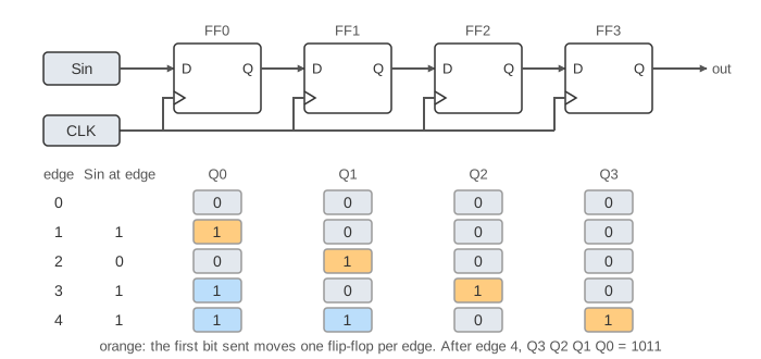
At the edge, FF1 copies D1 = Q0 while FF0 is changing Q0 at the same moment. It still gets the old Q0. A flip-flop samples D at the edge, and its own output changes only a short clock-to-Q delay later. So every flip-flop sees its neighbour's value from before the edge, and each bit moves exactly one place per edge, never two. The page shows this in two steps: first all four D values are taken, then all four Q outputs change. The new Q values reach the next D inputs at once, but they wait there for the next edge.
This only works if the clock reaches all flip-flops at nearly the same time. If one flip-flop's clock arrives late (clock skew), its neighbour may already show the new value, and a bit jumps two places. That is a hold-time failure; see Timing Analysis.
Serial in, parallel out
In the shift register, D0 comes from an input pin Sin. Send the bits 1, 0, 1, 1, one per clock edge, and after 4 edges Q0 Q1 Q2 Q3 = 1 1 0 1. Read from Q3 back to Q0 it is 1011, the order the bits were sent. The register has turned a serial stream into a parallel 4-bit word (Demo: shift in 1011). Q3 is also a serial output: each bit comes out 4 edges after it went in, so the register is also a 4-cycle delay line.
| kind | input | output | used for |
|---|---|---|---|
| SIPO (serial in, parallel out) | one bit per edge | all Q at once | a UART or SPI receiver collecting a byte |
| PISO (parallel in, serial out) | load all D at once | one bit per edge | a UART or SPI transmitter |
| SISO (serial in, serial out) | one bit per edge | the last Q | a delay of N clock cycles |
| universal | a mux before each D picks hold, shift left, shift right or load | both | the 74194 chip |
Counters from feedback
Take away Sin and feed the end of the chain back into D0. The register now steps through a fixed sequence of states on its own: a counter. What goes into D0 decides how long the sequence is.
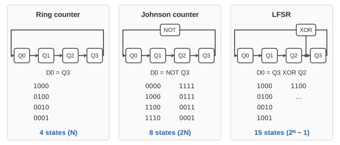
- Ring counter, D0 = Q3. Start with one 1 (1000) and the 1 goes round: 1000, 0100, 0010, 0001, 1000. N flip-flops give N states. Exactly one Q is 1 at a time (one-hot), so each state has its own wire and needs no decoder (Demo: ring counter).
- Johnson counter (twisted ring), D0 = NOT Q3. From 0000 the register fills with 1s from the left until 1111, then with 0s: 8 states, 2N from N flip-flops. Neighbouring states differ in one bit, so a decoder needs only a 2-input gate per state and gives no glitches (Demo: Johnson counter, 8 states).
- LFSR (linear-feedback shift register), D0 = Q3 XOR Q2. These taps belong to the polynomial x⁴ + x³ + 1, which is primitive, so the register visits all 2ᴺ − 1 = 15 non-zero states before it repeats. The order looks random, so LFSRs make test patterns (PRBS), scramble data on a link, and compute CRCs (Demo: LFSR, 15 states; see CRC).
The binary counter
A binary counter is not a shift register. It is a 4-bit register whose D inputs come from an incrementer: D = Q + 1. The page draws FF3 on the left so that Q3 Q2 Q1 Q0 reads as a binary number. At every edge the register loads its own value plus one: 0, 1, 2, … 15, then 1111 + 1 = 10000 does not fit in 4 bits and the counter wraps to 0000 (Demo: binary counter wraps). It uses all 2ᴺ = 16 states. Written out bit by bit, D0 = NOT Q0, D1 = Q1 XOR Q0, D2 = Q2 XOR (Q1 AND Q0), and so on: the carry ripples through the incrementer, which is why a wide counter needs a carry-lookahead for a fast clock (see Arithmetic Circuits).
| circuit | D0 | states with N = 4 | in general | logic needed |
|---|---|---|---|---|
| ring counter | Q3 | 4 | N | none |
| Johnson counter | NOT Q3 | 8 | 2N | one inverter |
| LFSR | Q3 XOR Q2 | 15 | 2ᴺ − 1 | one or a few XORs |
| binary counter | NOT Q0 (D = Q + 1) | 16 | 2ᴺ | an N-bit incrementer |
Bad states and reset
Flip-flops can come out of power-up in any state. A binary counter does not care: every one of its 16 states is part of the count. The feedback counters do. A ring counter loaded with 0000 has no 1 to pass round and stays 0000 forever (Demo: ring counter stuck at 0000). An LFSR at 0000 is stuck too, because 0 XOR 0 = 0. A Johnson counter uses only 8 of its 16 states, and the other 8 form a second loop of their own: from 0100 it goes 1010, 1101, 0110, 1011, 0101, 0010, 1001 and back to 0100, and never reaches a legal state (Demo: Johnson illegal loop).
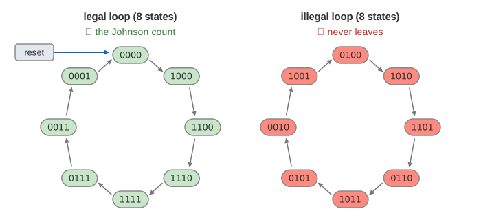
So real designs give these registers a reset that forces a known legal state (0000 for a Johnson counter, 1000 for a ring counter, any non-zero seed for an LFSR). Some designs also add self-correcting logic that steers an illegal state back into the main loop.
Where they are used
- Serial links (UART, SPI, I²C): a shift register on each side turns a byte into a bit stream and back.
- CRC and scramblers: an LFSR with the generator polynomial's taps, in Ethernet, USB, PCIe and SATA.
- Built-in self test: an LFSR makes test patterns; scan chains link every flip-flop of a chip into one long shift register.
- State machines: a one-hot state register is a ring counter with extra logic; see Finite State Machines.
- Timers, program counters and clock dividers are binary counters; Q0 of a counter is the clock divided by 2.
The flip-flop inside each box, built from gates with its setup and hold times, is on Sequential Logic.
What the page leaves out
- Time inside a clock cycle. Every flip-flop changes at once. Real ones have clock-to-Q, setup and hold times, and the incrementer has a carry delay that limits the clock rate.
- Ripple (asynchronous) counters, where each flip-flop is clocked by the previous Q. They are smaller but pass through wrong values while the bits change one after another.
- Parallel load, enable, shift direction and reset pins. The circuits here only shift or count; the demos set a power-up state directly.
- Galois LFSRs, longer polynomials and down or BCD counters.
On the mind map
References
Harris and Harris, Digital Design and Computer Architecture, sections 3.4 (synchronous sequential logic) and 5.4 (counters and shift registers)