The idea: DRAM reads a whole row at a time
Main memory is DRAM: each bit is a tiny capacitor behind a transistor, packed in a grid of rows and columns (a bank). The chip cannot read one cell on its own. It first copies a whole row into the row buffer, a line of sense amplifiers under the grid, and then picks columns out of that buffer. So whether the row you want is already in the buffer decides how long a read takes.
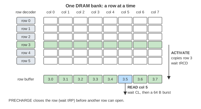
The canvas shows one bank with 8 rows of 8 cells, where one cell stands for one 64-byte cache line. A real DDR4 row is 8 KB, that is 128 such lines. On the left, the memory controller in the CPU keeps a queue of requests and sends commands over the command bus. The data comes back over the 64-bit data bus. The timeline under them draws each command, the wait after it, and every data burst.
ACTIVATE, READ and PRECHARGE
The controller talks to the bank with three commands. The old names come from the address being sent in two halves:
- ACTIVATE (RAS, row address strobe) sends the row number. The decoder raises that row's wordline, the cells share their charge with the bitlines, and the sense amplifiers turn it into full 0s and 1s. After tRCD the row is ready in the buffer.
- READ (CAS, column address strobe) sends only the column number. The first data appears on the pins CL (CAS latency) clocks later.
- PRECHARGE writes the row back into its cells and brings the bitlines back to half voltage, ready for the next row. That takes tRP. Only then can another row in the same bank be activated.
The page uses DDR4-2400 with 17-17-17 timings. The clock runs at 1200 MHz (tCK = 0.833 ns), and data moves on both edges, so 2400 transfers per second per pin.
| Timing | Clocks | Time | Between |
|---|---|---|---|
| tRCD | 17 | 14.2 ns | ACTIVATE → READ |
| CL | 17 | 14.2 ns | READ → first data |
| tRP | 17 | 14.2 ns | PRECHARGE → ACTIVATE |
| burst (BL8) | 4 | 3.3 ns | 8 transfers of 8 bytes |
| tCCD | 4 | 3.3 ns | READ → next READ in the same row |
| tRTP | 9 | 7.5 ns | READ → PRECHARGE |
| tRAS | 39 | 32.5 ns | ACTIVATE → PRECHARGE (cells restored) |
| tRFC | 192 | 160 ns | REFRESH → next command |
Row hit and row miss
If the row is already open, a read is a row hit: the controller sends only READ and waits CL plus the burst, 21 clocks = 17.5 ns (Demo: Row hit). If another row is open, it is a row miss: PRECHARGE, wait tRP, ACTIVATE, wait tRCD, READ, wait CL, then the burst. That is 55 clocks = 45.8 ns, about 2.6 times longer (Demo: Row miss). If the bank is already closed, for example after a refresh, the PRECHARGE is skipped: 38 clocks = 31.7 ns.
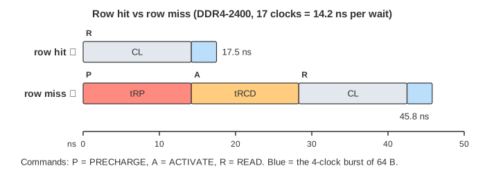
These are the latencies inside the DRAM. A load that misses every cache also pays for the trip through the caches, the on-chip network and the controller's queue, which is why a CPU sees 60 to 100 ns.
DDR bursts and bandwidth
One READ does not return one word. It returns a burst of 8 transfers (BL8) of 8 bytes each, one on every rising and every falling clock edge: that is the double data rate. 8 × 8 = 64 bytes, one cache line, in 4 clocks (3.3 ns). The burst zoom on the canvas lights up the 8 beats while a burst is on the bus.
Peak bandwidth is 2400 million transfers per second × 8 bytes = 19.2 GB/s per channel. The bus only gets near it when the bursts follow each other with no gap. In the same open row that works: the controller can send a READ every 4 clocks (tCCD) while the earlier READs are still waiting out their CL, so their bursts land back to back.
Sequential vs random
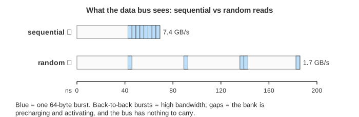
A sequential scan reads consecutive lines, and they sit in the same row. The first read is a miss, and the next seven are hits sent 4 clocks apart (Demo: Sequential scan of row 5). Random reads land in a different row almost every time. Each one pays PRECHARGE + ACTIVATE + READ, and tRAS keeps the row open at least 32.5 ns after its ACTIVATE, so a new row can open only about every 47 ns (Demo: Random reads).
| Demo | Reads | Time | Average latency | Bandwidth |
|---|---|---|---|---|
| Row hit | 1 hit | 17.5 ns | 17.5 ns | 3.66 GB/s |
| Row miss | 1 miss | 45.8 ns | 45.8 ns | 1.40 GB/s |
| Sequential scan | 7 hits, 1 miss | 69.2 ns | 21.0 ns | 7.40 GB/s |
| Random reads | 1 hit, 4 misses | 185.8 ns | 40.2 ns | 1.72 GB/s |
| Refresh | 6 hits, 2 misses | 262.5 ns | 44.6 ns | 1.95 GB/s |
A read's latency here runs from the first command sent for it to its last data beat. Bandwidth is the bytes moved divided by the time from the first command to the last beat. The scan's 7.4 GB/s is held back by its one miss. A scan of a whole 8 KB row (128 lines) takes 34 + 127 × 4 + 21 = 563 clocks for 8 KB: 17.5 GB/s, 91% of the peak. That is why code that walks arrays in order is so much faster than code that chases pointers. Caches and hardware prefetchers turn sequential access into exactly this pattern, and see How a CPU Cache Finds, Misses and Replaces for the cache side.
Refresh
A DRAM cell leaks its charge within milliseconds, so every row must be read and rewritten every 64 ms. The controller sends a REFRESH command about every 7.8 µs (tREFI). The bank must be closed first, and for tRFC (160 ns on a 2 Gb chip, 350 ns on an 8 Gb chip) it takes no other command (Demo: Refresh steals the bank). The read behind the refresh waits about 206 ns, and the open row has to be activated again afterwards. Over time refresh takes a few percent of the bank's time, more on bigger chips. Memory Arrays shows the DRAM cell, its destructive read and refresh at the circuit level.
Devices that read memory without the CPU see the same timings: Direct Memory Access (DMA) follows a network card writing packets into RAM.
Where a DRAM access sits among the TLB, the caches and the disk, with the cycles each level costs, is shown in One Load Through the Memory Hierarchy.
What the page leaves out
A real channel has several ranks, each with 16 banks in 4 bank groups. The controller keeps many rows open at once and overlaps commands across banks, within limits such as tRRD and tFAW. It also reorders its queue to serve row hits first (FR-FCFS), and it chooses an open-page or closed-page policy. It maps addresses so that consecutive lines spread over channels and banks. The page also leaves out writes and the bus turnaround between reads and writes, the on-die termination, the training of signal timing at boot, and power-down states. DDR5 adds two 32-bit subchannels per DIMM and bursts of 16.
References
Harris and Harris, Digital Design and Computer Architecture, Sections 5.5 (Memory Arrays) and 8.6 (Real-World Perspective: memory in a PC)